GDDR5X: Speicherkonfigurationen und Features
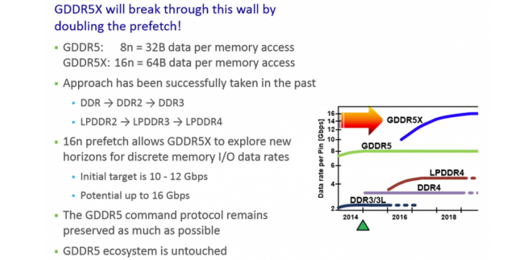
Bereits im November 2015 hat die JEDEC auf Bemühen von Micron den Speicherstandard GDDR5X spezifiziert. Das ging bislang unter, nichtsdestotrotz bietet die offizielle Spezifikation einige interessante Details. So wird unter anderem die maximal mögliche Speicherdichte verdoppelt, wodurch 2 GiByte pro Speicher-Package möglich werden. An 256 Bit könnte man so 16 GiByte hängen.
2 GDDR5X SGRAM Standard Overview
- 4 Gb = 128 Mb x 32 ( 8 Mb x 32 x 16 banks) / 256 Mb x 16 (16 Mb x 16 x 16 banks)
- 6 Gb = 192 Mb x 32 (12 Mb x 32 x 16 banks) / 384 Mb x 16 (24 Mb x 16 x 16 banks)
- 8 Gb = 256 Mb x 32 (16 Mb x 32 x 16 banks) / 512 Mb x 16 (32 Mb x 16 x 16 banks)
- 12 Gb = 384 Mb x 32 (24 Mb x 32 x 16 banks) / 768 Mb x 16 (48 Mb x 16 x 16 banks)
- 16 Gb = 512 Mb x 32 (32 Mb x 32 x 16 banks) / 1 Gb x 16 (64 Mb x 16 x 16 banks)
2.1 Features
• Single ended interface for command, address and data
• Differential clock input CK_t/CK_c for ADD/CMD
• Two differential clock inputs WCK_t/WCK_c, each associated with two data bytes (DQ, DBI_n, EDC)
• Single Data Rate (SDR) commands (CK)
• Double Data Rate (DDR) addresses (CK)
• QDR and DDR operating modes:
• QDR mode: Quad Data Rate (QDR) data (WCK); 16n prefetch architecture with 512 bit per array read or write access; burst length 16
• DDR mode: Double Data Rate (DDR) data (WCK); 8n prefetch architecture with 256 bit per array read or write access; burst length 8
• 16 internal banks
• 4 bank groups for tCCDL = 3 tCK and 4 tCK • Programmable read latency: 5 to 36 tCK; programmable write latency: 1 to 7 tCK • Write data mask function via address bus (single/double/quad byte mask)
• Data bus inversion (DBI) & address bus inversion (ABI)
• Input/output PLL/DLL
• Address training: address input monitoring via DQ/DBI_n/EDC pins
• WCK2CK clock training with phase information via EDC pins
• Data read and write training via READ FIFO (depth = 6)
• Read FIFO pattern preload by LDFF command
• Direct write data load to READ FIFO via WRTR command
• Consecutive read of READ FIFO via RDTR command
• Read/write EDC on/off mode
• Programmable EDC hold pattern for CDR
• Read/write data transmission integrity secured by cyclic redundancy check (CRC-8)
• Programmable CRC read latency = 1 to 4 tCK; programmable CRC write latency = 7 to 14 tCK • Low Power modes
• RDQS mode on EDC pins
• On-chip temperature sensor with read-out
• Auto & self refresh modes
• Auto precharge option for each burst access
• Temperature sensor controlled self refresh rate
• Optional digital tRAS lockout
• On-die termination (ODT) for all high-speed inputs
• Pseudo open drain (POD-135) compatible outputs
• ODT and output driver strength auto-calibration with external resistor ZQ pin (120 Ω)
• Programmable termination and driver strength offsets
• Internal VREF for data inputs with programmable levels
• Selectable external or internal VREF for address / command inputs
• Vendor ID for device identification
• Mirror function with MF pin
• IEEE 1149.1 compliant boundary scan
• 1.35 V supply voltage for device operation (VDD) and I/O interface (VDDQ)
• 1.8 V pump voltage (VPP)
• 190 ball BGA package

 )
) )
)


Von daher würde ich es als notwendig ansehen, wenn man da auf das modernere DDR4 äquivalent setzen würde (evtl ja mit DDR4-2133-, also unterclocked, da die Leistung ausreichen würde und man noch mehr Strom mit sparen würde
Ansonsten freuen ich mich aber darauf, was da so alles schönes mit GDDR5X und HBM2 gezaubert werden wird